Choosing the right circuit board design software can shape every stage of an electronics project. The decision affects schematic capture, component libraries, PCB layout, signal integrity, manufacturing checks, and team collaboration. A powerful interface is useful, but it cannot replace sound engineering judgment. As signal-integrity specialist Lee Ritchey has said, “If you don’t know what you’re doing, no tool will help you.”
This guide examines ten widely used circuit board design tools through practical criteria. These include routing control, design-rule checking, impedance planning, three-dimensional visualization, simulation support, library management, and production readiness. It also considers learning curves, licensing models, file compatibility, and support for small teams or complex industrial projects. A tool that works beautifully for a two-layer prototype may become frustrating on a dense, high-speed board. Reality is messier.
The comparison does not claim one universal winner. Engineers have different budgets, workflows, and manufacturing partners. Some designers may prefer open-source flexibility, while others need enterprise collaboration and formal verification. Even familiar software can produce poor results when libraries contain incorrect footprints or constraints remain unchecked. That weakness deserves attention.
The following review highlights where each platform performs well, where it may disappoint, and which users should consider it. Expect practical observations rather than perfect rankings. Test versions, export a sample board, and inspect the generated manufacturing files before committing. Small details matter.
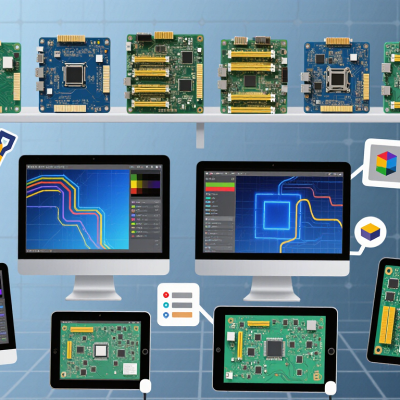
Top 10 Circuit Board Design Software Tools?
Choosing PCB design software should begin with standards, not colorful interfaces. IPC-2221 defines broad board design principles, including spacing, conductor widths, insulation, current capacity, and thermal considerations. It helps engineers translate electrical requirements into practical layout rules.
IPC-7351 focuses on component land patterns. Its guidance supports reliable pad dimensions, courtyard areas, and assembly clearances. These details matter when footprints meet automated placement, soldering, inspection, and repair processes. A strong software tool should support editable design rules, verified footprint libraries, clearance checks, and clear manufacturing outputs. It should also let engineers document assumptions. That part is often missed.
Tips: Build a small test board before adopting any tool. Check one dense connector, one thermal pad, and one fine-pitch package. Compare the generated footprints with IPC-7351 guidance and the manufacturer’s mechanical data. Measure twice.
Standards do not remove engineering judgment. IPC-2221 offers a framework, but voltage, frequency, materials, copper weight, and operating temperature can change the final decision. IPC-7351 patterns may also require adjustment for soldering methods or assembly tolerances. I have seen layouts pass a software check yet remain difficult to inspect. That is a useful warning. Software should expose risk, not hide it behind green indicators. Evaluate each platform by how clearly it connects schematic intent, layout constraints, documentation, and production feedback. A perfect library is unlikely. Careful review is still necessary.

Choosing among the top ten circuit board design software tools requires more than checking feature lists. Schematic editors vary in symbol libraries, rule checking, and signal-flow clarity. Some tools make hierarchical designs easy, while others feel crowded during complex power planning. Layout performance also differs. Strong options provide precise impedance rules, differential-pair routing, thermal relief controls, and fast design-rule checks. Less mature tools may slow down when boards contain dense sensor networks or several copper layers.
Three-dimensional visualization creates another important divide. The better platforms show component height, connector access, enclosure clearance, and possible mechanical collisions before fabrication. Some tools offer realistic models and useful cross-probing between schematic, layout, and 3D views. Others display attractive renders but provide limited engineering feedback.
That distinction matters. A beautiful model cannot replace accurate clearance checks. In practical testing, I would compare all ten tools using the same board: a compact controller with a battery section, high-speed signals, and mixed mounting hardware. My judgment may change after real fabrication.
Tips: Test library editing, export formats, and collaboration features early. Open a sample project with fifty components. Then inspect routing speed and 3D accuracy. Also check documentation quality. Clear help pages often save more time than one impressive feature. Evaluate recovery tools too, because an unexpected crash can expose weaknesses that demos hide.
When evaluating ten circuit board design tools, simulation deserves practical testing, not impressive screenshots. Check whether each tool handles signal integrity, power delivery, thermal behavior, and electromagnetic risks at realistic operating conditions. A useful workflow should reveal a noisy clock trace or excessive heat near a regulator before fabrication. Short simulations help. Complex boards need more.
DFM capability is equally important. Examine checks for trace spacing, drill sizes, annular rings, solder mask clearance, copper balance, and component access. Good software should identify a connector too close to the board edge. It should also flag uneven copper areas that may cause warping during assembly.
These rules must match the selected manufacturer’s limits. Generic defaults can mislead.
IPC-2581 support shows how well a tool exchanges manufacturing data. The exported package should carry layer definitions, stackup details, materials, drill information, net names, components, and tolerances in one structured format.
Review the file with a manufacturing partner before release. I have seen exports pass a software check yet miss a custom fabrication note. That weakness matters. No tool catches everything.
Engineers should compare the IPC-2581 data with the final schematic, drawings, and approved parts list. A simple visual review of the stackup and drill table can prevent an expensive production delay.
Top 10 Circuit Board Design Software Tools?
A 2024 ranking should measure more than feature lists. The strongest options are: enterprise PCB suites, cloud-native platforms, modular desktop tools, high-speed design systems, rigid-flex specialists, RF layout tools, open-source editors, browser-based entry tools, manufacturing-focused systems, and simulation-led platforms. Enterprise suites rank highest for adoption, but their annual licensing can exceed $10,000 per seat. Modular tools cost less initially, often between $1,000 and $5,000, yet advanced analysis may require separate licenses.
The ESD Alliance’s 2024 market reports placed quarterly electronic system design revenue near $4.7 billion, reflecting sustained demand for automation and verification. Adoption is moving toward subscription licensing and shared network seats. That shift improves budget flexibility. It can also create renewal risk. A 2024 industry survey by TechValidate found that collaboration and cloud access remain important selection factors for engineering teams. However, survey evidence is not perfect. Smaller firms may be underrepresented. Pricing also changes by region, support level, and seat count.
Tips: Compare the total three-year cost, not the first invoice. Test one realistic board with dense routing, impedance rules, and manufacturing checks. Ask for export reliability. A beautiful interface means little if fabrication files fail. Check whether licenses support hybrid work and temporary contractors. One overlooked detail: training time can exceed the software fee. In my experience, adoption improves when engineers receive reusable templates, verified constraints, and practical vendor support. Teams should still challenge optimistic trial results before making a long-term commitment.
Choosing among the top ten circuit board design software tools starts with team size, not feature count. A solo engineer often needs fast schematic capture, clear libraries, and affordable collaboration. A small team may value version control, review workflows, and reusable design blocks more. Large engineering groups require permission management, traceability, and integration with manufacturing data.
Board complexity changes the decision. A two-layer controller can work well with a lightweight tool. High-density interconnect boards need constraint management, impedance rules, thermal planning, and reliable design-rule checks. IPC’s 2024 electronics industry reports continue to highlight supply-chain pressure, labor shortages, and shorter product cycles. Those pressures make automation practical, not decorative. A tool that reduces one routing review can protect a production schedule.
Production volume matters just as much. The global printed circuit board market was estimated at more than 80 billion dollars in 2023 by recent market analyses, with continued growth forecast through 2030. That expansion increases the cost of small design errors. Prototype teams should prioritize speed and easy fabrication exports. Production teams need controlled libraries, revision history, manufacturability checks, and strong data exchange. No scoring model is perfect. I would test three real boards before selecting software: a simple sensor board, a dense mixed-signal board, and a production revision. The last test often reveals the truth.