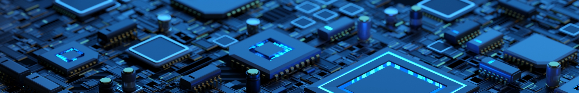
The Future of PCB Design Innovations You Need to Know About
As the electronics industry continues to evolve, the landscape of PCB design is undergoing significant transformations driven by advancements in technology and increasing demands for efficiency and miniaturization. According to a recent report by ResearchAndMarkets, the global PCB market is projected to reach $78.4 billion by 2026, growing at a CAGR of 4.2%. This growth underscores the urgent need for innovative PCB design strategies that not only enhance performance but also cater to the complexities of modern electronic devices. With developments in areas such as AI-integrated design software and flexible PCB technologies, designers are now equipped with powerful tools that can streamline workflows and improve precision. As we delve into the future of PCB design, understanding these innovations is crucial for staying competitive in a rapidly changing market.
Emerging Technologies Shaping the Future of PCB Design
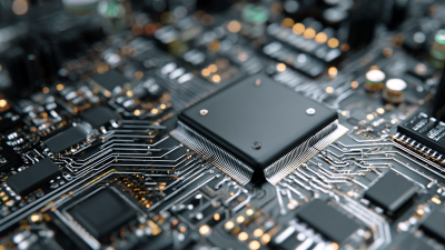
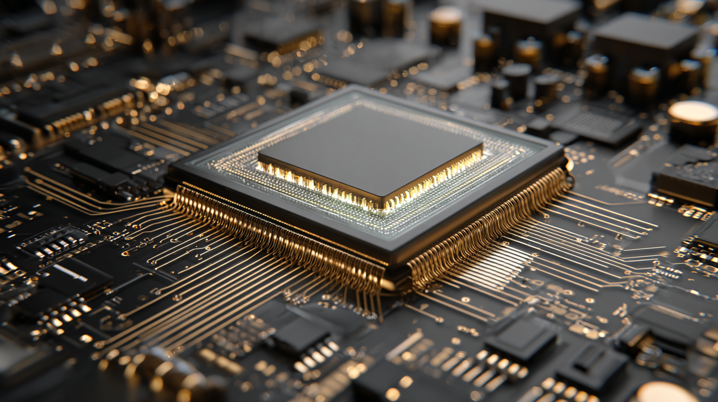
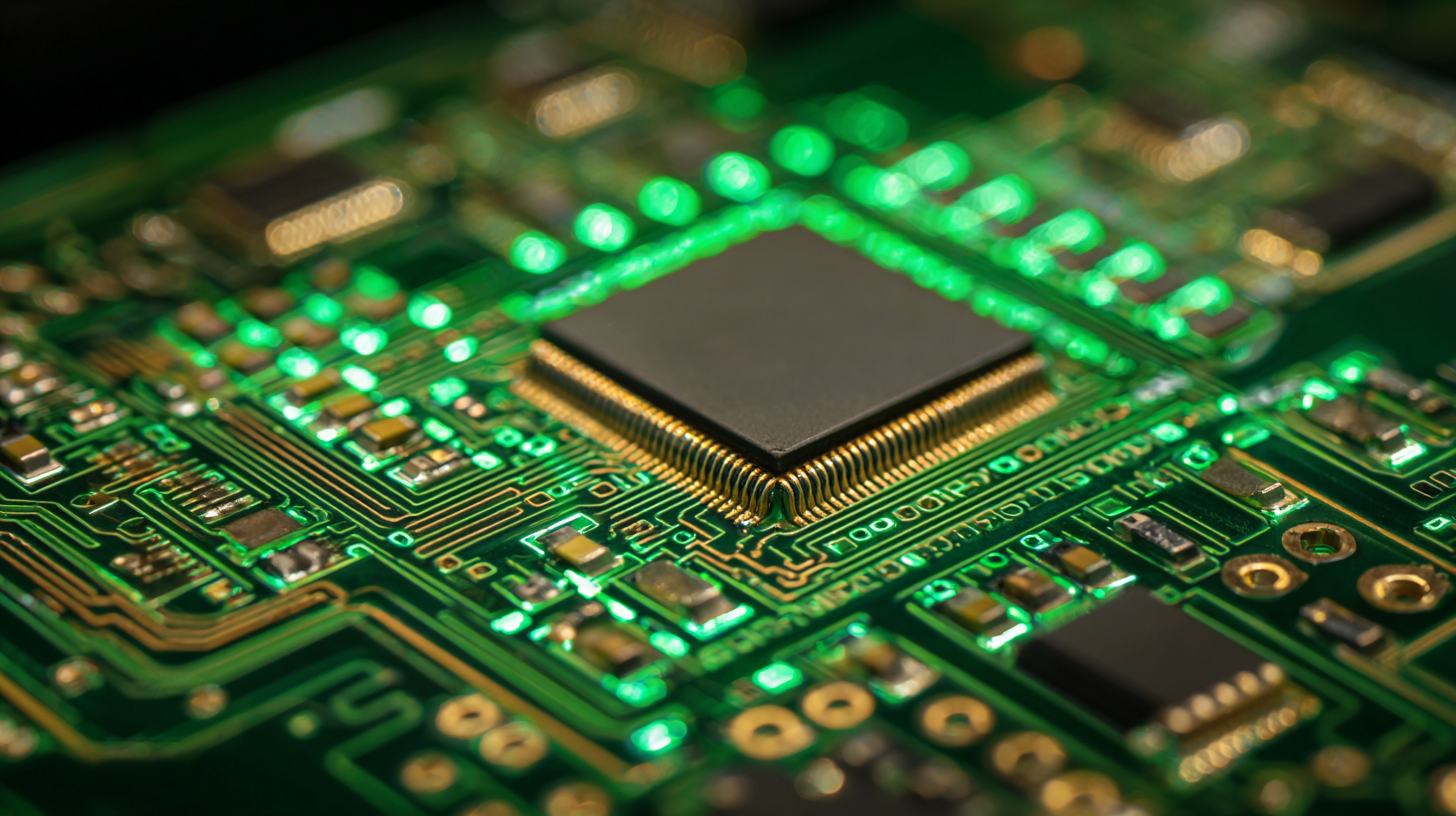
As the world progresses towards greater connectivity and miniaturization, emerging technologies are reshaping the landscape of PCB design. One of the most significant innovations is the rise of additive manufacturing techniques, such as 3D printing, which allow for the rapid prototyping and production of complex PCB structures. This method not only accelerates the design process but also enables engineers to create intricate circuit layouts that were previously unfeasible. As a result, the ability to customize PCBs to meet specific application requirements has skyrocketed, providing a competitive edge in industries ranging from consumer electronics to automotive applications.
In addition to additive manufacturing, developments in materials science are playing a crucial role in the evolution of PCB design. Advanced materials like flexible substrates and high-frequency laminates are allowing for more versatile and efficient board designs. These materials not only improve the performance of electronic devices but also facilitate the integration of multiple functionalities onto a single board, thus reducing size and weight. Furthermore, the integration of AI-driven design tools is streamlining the design process, helping engineers optimize layouts and identify potential issues before physical production begins. Together, these technologies are paving the way for a more innovative and efficient future in PCB design.
Sustainable Practices in PCB Manufacturing and Design Innovations
Sustainable practices in PCB manufacturing and design are becoming increasingly vital as industries strive to reduce their environmental impact. Innovations in materials, such as biodegradable substrates and lead-free solder, are paving the way for greener circuits. These advancements not only minimize toxic waste but also enhance the recyclability of PCBs. By integrating sustainable materials into the design process, manufacturers can significantly lower their carbon footprint while meeting the rising demand for eco-friendly products.
Another key aspect of sustainability in PCB design is the implementation of efficient manufacturing processes. Techniques such as additive manufacturing, or 3D printing, allow for more precise material usage and less waste generation. By optimizing layout designs and incorporating modular components, engineers can create PCBs that are easier to repair and upgrade, extending the lifespan of electronic devices. Overall, the future of PCB design innovations is firmly rooted in sustainable methodologies, promising both environmental benefits and economic efficiency for manufacturers and consumers alike.
Leveraging AI and Machine Learning for Enhanced PCB Development
As the landscape of PCB design evolves, the integration of Artificial Intelligence (AI) and Machine Learning (ML) stands out as a transformative force. These advanced technologies streamline the design process, reduce human error, and enhance overall efficiency. By automating routine tasks, designers are freed to focus on more complex challenges, thus accelerating innovation in circuit board development.
**Tip:** Embrace the use of predictive analytics within your design tools. By analyzing past designs and their performance, AI can suggest improvements and identify potential issues before they manifest. This ability not only speeds up the design cycle but also fosters the creation of more reliable and effective PCBs.
Moreover, AI algorithms can optimize layout designs by enhancing component placement and routing efficiency. Machine learning models trained on vast datasets can determine the most effective configurations, facilitating better performance with minimal space.
**Tip:** Regularly update your AI and ML models with new data from your projects. This continuous learning approach ensures that your tools remain current and can adapt to new trends and technologies, ultimately leading to superior PCB designs.
The Role of 3D Printing in Revolutionizing PCB Prototyping
As the electronics industry evolves, 3D printing emerges as a game-changer in PCB prototyping. This innovative technology reduces the time required to create prototype boards significantly, enabling faster iterations and a more efficient design process. According to a recent report by IDTechEx, the global market for 3D printed electronics is expected to reach $1.5 billion by 2027, reflecting the growing adoption of additive manufacturing in electronics applications. This shift not only enhances design flexibility but also caters to the demand for custom and complex geometries that traditional manufacturing methods struggle to achieve.
Moreover, 3D printing facilitates a more sustainable approach to PCB production. By minimizing material waste and allowing for on-demand production, it effectively addresses the environmental concerns associated with traditional PCB manufacturing, which is notorious for its high waste output. Research from the International Journal of Advanced Manufacturing Technology indicates that 3D printing can reduce material costs by up to 50%, highlighting its potential to reshape the financial landscape of PCB prototyping. As a result, the integration of 3D printing into PCB design processes is poised to redefine the future of electronic manufacturing, streamlining operations while promoting eco-friendly practices.
Integrating IoT Solutions into Next-Generation PCB Designs
The integration of IoT solutions into next-generation PCB designs is revolutionizing the electronics landscape. As the demand for smart devices continues to rise, PCB designers are increasingly focusing on embedding IoT technologies to enhance functionality and connectivity. According to a report by MarketsandMarkets, the global IoT market is expected to grow from $384.5 billion in 2021 to $1,463 billion by 2027, showcasing an annual growth rate of over 25%. This surge is driving innovations in PCB design, allowing for more compact, efficient, and interconnected devices.
Incorporating IoT requires a shift in PCB design paradigms. Designers must consider aspects such as antenna placement, miniaturization, and power management to ensure optimal performance. For instance, smart sensors and wireless communication modules need to be seamlessly integrated, often leading to multilayer designs that save space while accommodating complex functionalities.
**Tips:** When designing PCBs for IoT applications, consider using advanced simulation tools that can predict how various components will interact. Additionally, keep power consumption in mind; using low-power components can significantly extend the lifespan of battery-operated devices. Lastly, always plan for scalability in your designs to adapt to future technological advancements.
The Future of PCB Design Innovations You Need to Know About - Integrating IoT Solutions into Next-Generation PCB Designs
| Innovation |
Description |
Impact on PCB Design |
IoT Integration |
| Flexible PCB Technology |
Use of flexible materials to create bendable circuit boards |
Increased design versatility for compact devices |
Supports wearable technologies and IoT devices |
| 3D Printing in PCB Manufacturing |
Additive manufacturing techniques for creating PCBs |
Reduced production costs and shorter lead times |
Allows rapid prototype development for IoT devices |
| Advanced Thermal Management |
Innovations in heat dissipation technologies |
Enhanced performance and lifespan of PCBs |
Critical for IoT devices with high power consumption |
| Embedded Components |
Integration of components directly into the PCB substrate |
Saves space and improves reliability |
Ideal for compact IoT devices |
| AI-Driven Design Tools |
Software utilizing AI to optimize PCB layouts |
Increased efficiency and design accuracy |
Facilitates complex IoT system designs |